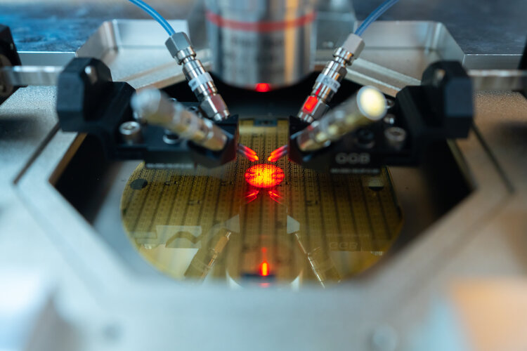
As a ‘wide bandgap’ semiconductor, GaN can operate at much higher voltages and temperatures than traditional materials such as silicon or gallium arsenide. It was first commercially employed in the 1990s as an energy-efficient method of generating blue light.
Today – as silicon-based power devices move towards the limit of their operating temperature, breakdown voltage and power density – GaN is increasingly favoured for Radio Frequency (RF) signal amplification as well as very high power switching systems.
ESA’s ESTEC technology centre in the Netherlands recently oversaw lifetime testing of GaN-based high-power amplifier monolithic microwave integrated circuits (MMICs), the basis of a Dual Solid State Power Amplifier design being developed by SENER in Spain through ESA’s PACIS3 Partnership Project, set to operate aboard a pair of next generation Hisdesat telecom satellites, due to launch in 2023-4.
“These integrated circuits rely on a state of the art 0.25 μm gate length GaN technology from United Monolithic Semiconductors,” comments ESA engineer Václav Valenta who supports various developments of active antenna payloads. “This means the transistor gate terminals are fabricated onto the Gallium Nitride semiconductor chips to a size of 0.25 micrometres – a micrometre being a thousandth of a millimetre.


